Copyright © 2019 深圳市蓝星宇电子科技有限公司 All Rights Reserved 粤ICP备2025493771号


|
P-SPL21 德国针尖电子束光刻系统
咨询购买
|
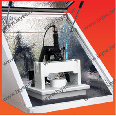
德国针尖电子束光刻系统 P-SPL21
ParcanNano 公司以全球独家专利的针尖技术为核心竞争力,技术源自于德国伊尔默瑙工业大学,致力于主动式针尖技术在微纳米结构制备和表征方面的研发,及其相关设备的产业化。公司研制一套基于扫描针尖低能电子场发射的原理、采用压阻式微纳米针尖和多维纳米定位与测量技术、在半导体器件材料表面制造尺寸小于5纳米线宽结构的高性能微纳加工系统。公司致力于为微纳米制造企业提供制备微纳米功能结构和功能器件(比如最高速且最省电的基于单电子器件的芯片)的高性能设备和技术服务。

利用探针在近光刻胶表面发射低能电子的原理实现光刻效果。该系统的主要特点在于:
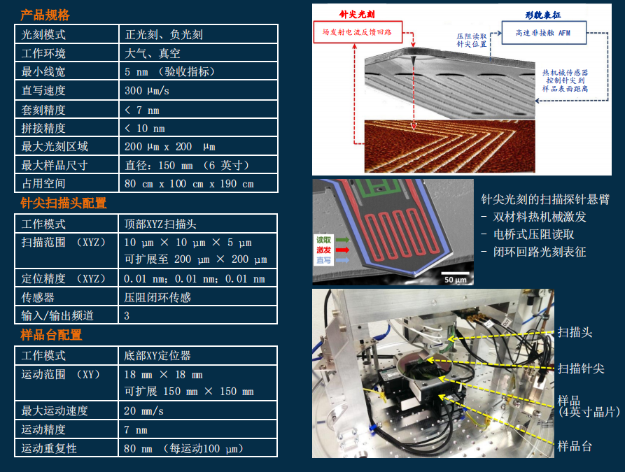
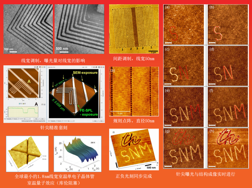
(1)几乎无邻近效 应,能实现 3-5nm 线宽的超精细光刻结构;
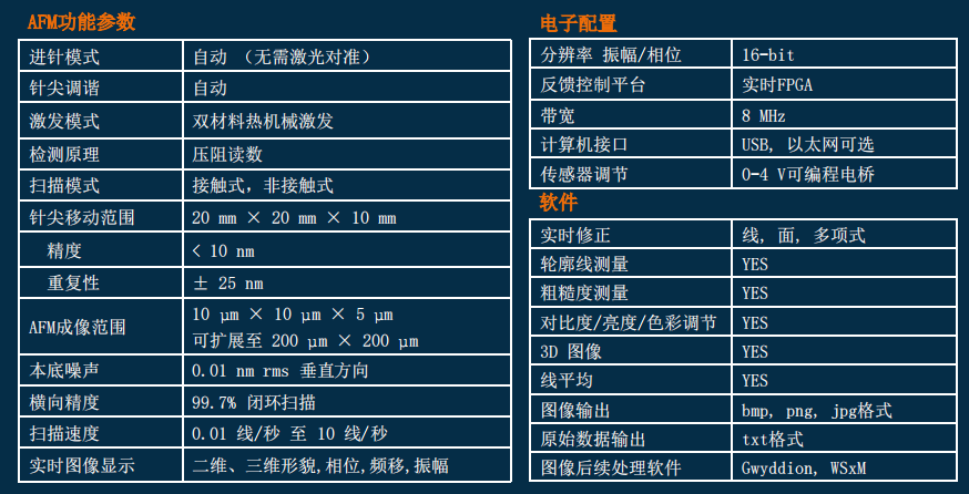
(2)用于发射电子的探针同时具有原子力显微镜功能,能够实现亚纳米级精准定位并原位测量曝光图型;
(3)超高写场拼接精度(≤2nm),且能够抑制电子束长时间产生的空间漂移(≤5nm)。百及纳米科技的探针电子束光刻系统能够实现光刻与原子力 显微镜表征的双重功能,是一款理想的用于微纳制造和表征尺寸小于 5nm 线宽结构的一体化系统。
尤其是针对二维材料,探针的电子束场发射可以直接辐照在二维材料(如 MoS2,石墨烯等)表面形成感光反应,去除曝光区的二维材料,直接显影并呈现出预设的超精细结构,达到无需使用电子束光刻胶而直接转移图形的效果。

A single probe electron beam lithography system P-SPL21
The lithography effect is achieved by the low energy electron emission from the probe near the photoresist surface. The main characteristics of the system are:
(1) With almost no proximity effect, the hyperfine lithography structure with a linewidth of 3-5nm can be realized;
(2) The probe used for emitting electrons also has the function of atomic force microscopy, which can realize accurate positioning and in situ measurement of the exposure pattern at the sub-nanometer level;
(3) Ultra-high write field stitching accuracy (≤2nm), and can suppress the spatial drift generated by the electron beam for a long time (≤5nm). B&n's probe electron beam lithography system can realize the dual function of lithography and AFM characterization. It is an ideal integrated system for micro-nano fabrication and characterization of structures with linewidth less than 5nm.
Especially for two-dimensional materials, the electron beam field emission of the probe can directly irradiate the surface of two-dimensional materials (such as MoS2, graphene, etc.) to form a photosensitive reaction, remove the two-dimensional materials in the exposure area, directly develop and present the preset hyperfine structure, so as to achieve the effect of directly transferring the pattern without using electron beam photoresist.
Copyright © 2019 深圳市蓝星宇电子科技有限公司 All Rights Reserved 粤ICP备2025493771号
咨询电话
廖经理 13538131258

